पाठ-३,अभियान्त्रिकरण (Electronics) -


2. Title
: Encoder
Block
diagram


 Closed loop voltage gain

Understanding
4-to-1 Multiplexer:

Applications
of Multiplexer:
2.Title
- Demultiplexer

3.use 1-
to-4 Demultiplexer:


…….Bharatpur Chitwan
Practical lesson 3
Date:
class: Electronics experiment
no:
Roll no: shift
or group:
1 . Title :Full Adder
Tools and materials :
Kit
prove
Procedure : connection manual instruction and teacher
guide.
Theory:
This type of adder is a little more difficult to implement than
a half-adder. The main difference between a half-adder and a full-adder is that
the full-adder has three inputs and two outputs. The first two inputs are A and
B and the third input is an input carry designated as CIN. When a full adder
logic is designed we will be able to string eight of them together to create a
byte-wide adder and cascade the carry bit from one adder to the next.
Output /observation:
The output carry is designated as COUT and the normal output is
designated as S. Take a look at the truth-table.
INPUTS
OUTPUTS
A
B
CIN
COUT S
0
0
0
0
0
0
0
1
0
1
0
1
0
0
1
0
1
1
1
0
1
0
0
0
1
1
0
1
1
0
1
1
0
1
0
1
1
1
1
1
From the above truth-table, the full adder logic can be implemented.
We can see that the output S is an EXOR between the input A and the half-adder
SUM output with B and CIN inputs. We must also note that the COUT will only be
true if any of the two inputs out of the three are HIGH.
Thus, we can implement a full adder circuit with the help of two
half adder circuits. The first will half adder will be used to add A and B to
produce a partial Sum. The second half adder logic can be used to add CIN to
the Sum produced by the first half adder to get the final S output. If any of
the half adder logic produces a carry, there will be an output carry. Thus,
COUT will be an OR function of the half-adder Carry outputs. Take a look at the
implementation of the full adder circuit shown below.
Full Adder Circuit
Though the implementation of larger logic diagrams is possible
with the above full adder logic a simpler symbol is mostly used to represent
the operation. Given below is a simpler schematic representation of a one-bit
full adder.
Single-bit Full Adder
With this type of symbol, we can add two bits together taking a
carry from the next lower order of magnitude, and sending a carry to the next
higher order of magnitude. In a computer, for a multi-bit operation, each bit
must be represented by a full adder and must be added simultaneously. Thus, to
add two 8-bit numbers, you will need 8 full adders which can be formed by
cascading two of the 4-bit blocks. The addition of two 4-bit numbers is shown
below.
Multi-Bit Addition using Full Adder
2. Title
: Encoder
Tools and materials :
Kit
prove
Procedure : connection manual instruction and teacher
guide.
Theory:
Encoder is a combinational
circuit which is designed to perform the inverse operation of the decoder. An
encoder has n number of input lines and m number of output lines. An encoder
produces an m bit binary code corresponding to the digital input number. The
encoder accepts an n input digital word and converts it into an m bit another
digital word.
Block
diagram
Examples of Encoders are
following.
·
Priority encoders
·
Decimal to BCD encoder
·
Octal to binary encoder
·
Hexadecimal to binary encoder
A decoder is a circuit that changes a code
into a set of signals. It is called a decoder because it does the reverse of
encoding, but we will begin our study of encoders and decoders with decoders
because they are simpler to design.
A common type of decoder
is the line decoder which takes an n-digit binary number and decodes it into 2ndata
lines. The simplest is the 1-to-2 line decoder. The truth table is
A is the address and D is the dataline. D0 is NOT A and D1 is A. The circuit looks like
Only slightly more complex is the 2-to-4 line
decoder. The truth table is
Developed into a circuit it looks like
Larger line decoders can be designed in a
similar fashion, but just like with the binary adder there is a way to make
larger decoders by combining smaller decoders. An alternate circuit for the
2-to-4 line decoder is
Replacing the 1-to-2 Decoders with their
circuits will show that both circuits are equivalent. In a similar fashion a
3-to-8 line decoder can be made from a 1-to-2 line decoder and a 2-to-4 line
decoder, and a 4-to-16 line decoder can be made from two 2-to-4 line decoders.
You might also consider making a 2-to-4 decoder
ladder from 1-to-2 decoder ladders. If you do it might look something like
this:
For some logic it may be required to build up
logic like this. For an eight-bit adder we only know how to sum eight bits by
summing one bit at a time. Usually it is easier to design ladder logic from
boolean equations or truth tables rather than design logic gates and then
“translate” that into ladder logic.
A typical application of a line decoder
circuit is to select among multiple devices. A circuit needing to select among
sixteen devices could have sixteen control lines to select which device should
“listen”. With a decoder only four control lines are needed.एडर
End
Subject: EDCblogger.g?
1.Title: op- amp
Object:
To
study op-amp as non inverting amplifier.
Apparatus need:
·
operation
amplifier kit
·
Patch
cord
·
Power
supply
Theory:
When
supply is given in non inverting terminals of Op Amp i.e. on the positive
terminals. Then it is called non inverting operational amplifier (op-amp). The
output is applied back to the input through the feedback circuit formed by
feedback resistance Rf and input resistance Ri . resistor Rf and Ri form a
voltage divide at the inverting input. this procedures product will negative feedback in the circuit.
Acl=
V Out /Vin = ( 1+ Rf / Ri)
figure
Observation
table:
V
in
|
Rf
|
Ri
|
Vout
= Vin x
(
1+ Rf / Ri )
|
1
v
|
10
k ohms
|
10
k ohms
|
2
v
|
2v
|
10
k ohms
|
10
k ohms
|
4
v
|
2.5v
|
10
k ohms
|
10
k ohms
|
5
v
|
3.02
v
|
10
k ohms
|
22
k ohms
|
4.32
v
|
3.02
v
|
22
k ohms
|
32
k ohms
|
5.07
v
|
Result:
In
this way property of an op amp as non inverting amplifier is studied.
Precautions:
·
Connection
should be tight
·
Precise
value of resistance and input voltage should be used for precise output
·
Connections
should made casualty to aboard electric shock.
End
2 . title : application of op- amp
Object: to verify op-amp
as summing amplifier.
Apparatus need:
·
operation
amplifier kit
·
Patch
cord
·
Power
supply,220 v
Theory:
Adder
circuit provides an output equal to the sum of these input signals with this
property of an amplifier is studied using the minimum value of resistance equal
to 10 k ohm's and 0 ohms.the output voltage
is equal to Vo= 10 ( V1+V2 )
V
Out = - Rf /R ( V1 + V2 )
figure
Observation table:
S n
|
V in 1
|
V in 2
|
Rf
|
R(k ohm's)
|
V Out = - Rf /R ( V1 + V2 )
|
1
|
2
v
|
2
v
|
10
k ohms
|
10
k ohms
|
3
v
|
2
|
3v
|
4v
|
22
k ohms
|
10
k ohms
|
15.4
v
|
3
|
2v
|
3v
|
33
k ohms
|
10
k ohms
|
16.5
v
|
4
|
3
v
|
3
v
|
33
k ohms
|
10
k ohms
|
9
v
|
5
|
4.5
v
|
4
v
|
10
k ohms
|
10
k ohms
|
3.86
v
|
Result:
We
can observe the output proportional to the sum of two input signal.
In
this way op-amp acts as adder in circuit.
Precaution:
·
Connection
should be tight
·
Precise
value of voltage and resistor should be made for precise output.
End
3.title : rectifier
Object: To verify the
characteristics of half wave rectifier
Apparatus need:
·
Diode
·
Resistor
·
Oscilloscope
·
node
Theory:
A
single phase shift wave rectifier is the simplest type of rectifier but it is
used in industrial application. The circuit diagram of the resistive load
half-wave rectifier is shown in the figure below the +v e half cycle of input
voltage. Diode, D1, is forward biased and conductor input voltage across the
load during the –ve half cycle of input voltage. Diode,D1, is reversed biased
hence, no current flows from the circuit and output voltage is zero.
Conclusion:
We
can easily rectify half wave the Ac by using the diode and use easily
understand it's characteristics.
end
4.title : rectifier(wave)
Object: To verify the
characteristics of full wave rectifier
Apparatus need:
·
Diode
·
Resistor
·
Oscilloscope
·
node
Theory:
A
full wave rectifier circuit with a center tapped transformer is shown in the
fig. below. Each half of transformer with its associated diode acts as a half
wave rectifier and output a full wave rectifier for positive half cycle of the
input voltage. Diode,D1 , conduct so the diode and transformer acts as a half
rectifier for the negative half cycle of the input voltage diode, D2, conduct.
When Diode, D2, is off condition so the diode D2 and transformer acts as half
wave rectifier.
Hence,
it gives output for both half cycle and known as full wave rectifier.
Conclusion:
We
can easily rectifier full wave the AC by using the diode and we can easily
understand it's characteristics.
End
Subject: Integrated Digital Electronics IDE object of experiment:
1.Title :
DIODE (BJT) AS A SWITCH
Object: BIPOLAR JUNCTION
DIODE (BJT) AS A SWITCH
Apparatus Requirements:–
·
Bread
board or pc board
·
Transistor
·
Resistor
·
LED
·
Battery
·
Jumper
wire
·
Power
supply
Theory:
Consider
an NPN transistor with a base resistor (rb)and collector (rc) as given figure.
Let
vcc be the supply voltage through collector terminals.
Figure
Procedure:
When
the base input voltage (vb) is zero or negative the transistor is in off state.
So the base current (ib) is zero and thus collector current (Ic) is equal to
collector leakage current (Iceo) but ideally this leakage current is negligible
[Ic=Iceo=C] .and hence there is no voltage drop across collector resistor (R)
.the output voltage ( v out) is idally equal to vcc ie (v out=v cc).
When
the base input voltage is positive enough that the transistor saturates i.e. it
turns in to ON state. In this condition the entire Vcc drops across the
colletor resistor(Rc) and the output
voltage is ideally equal to zero. i.e Ic = Ic(sat) = Vcc/Rc and Vout = 0.
Conclusion:
From
the experiment, it is clear that BJT can be act as a switch by driving base
current in high or low configuration.
END
2. Title :
DDL
OBJECT: TO REALISE AND VERIFY DDL
Apparatus
Required:
a.
Training Kit
b.
Probe
c.
Power supply
Theory:
DDL( Diode Diode Logic ) is also called
resistor diode logic. In this logic family all the logical functions are
performed using diode and register. Only the non inverting logical OR and
Logical and can be realized using this family.
Lab circuit design:
Fig:
Observation Table:
A
|
B
|
Z
|
0
|
0
|
0
|
0
|
1
|
1
|
1
|
1
|
1
|
1
|
1
|
1
|
Conclusion:
DDL circuit verifies the performance of
logic gate as shown. NAND and NOR gates
can also be obtained by simply connection respective gate to the NOR gate. Thus
verifying DDL circuit.
End
3.Title
: RTL
OBJECT: TO REDUCE OR
REALISE AND VERIFY RTL
Apparatus
Required:
a.
Training kit
b.
Probe
c.
Power supply
Theory:
In this logic family all the logical
operations are performed using transistor and resistor. The resistors are used
to input networks an transistors are used as a switching device. The RTL
circuit performing various operations shown as.
Lab circuit design:
Fig
Observation
table:
Input A
|
Input B
|
Output y= (a.b)'
|
0
|
0
|
0
|
0
|
1
|
0
|
1
|
0
|
0
|
1
|
1
|
1
|
Fig
Input A
|
Input B
|
Output y= (a.b)'
|
0
|
0
|
0
|
0
|
1
|
1
|
1
|
0
|
1
|
1
|
1
|
1
|
Conclusion:
RTL circuit verifies the performance of
logic gates as shown NAND and NOR gates can also be obtained by simply
connection respective gate to the NOR gate. Thus verifying RTL circuit.
End
4.Title : DTL
OBJECT: TO REALISE AND VERIFY DTL
Apparatus
Required:
a.
Training kit
b.
Power supply
c.
Probes
Theory:
In this logic family
all the logic operations are performed using diode, resistor and transistor. In
DTL, the logical gating function is
performed by using diode circuit and amplifying function is performed using
transistor. This logic family can be performed NAND gate operation. This
circuit below shows the operations of basic gates performed by DTL.
Input A
|
Input B
|
Output y= (a.b)'
|
0
|
0
|
1
|
0
|
1
|
1
|
1
|
0
|
1
|
1
|
1
|
0
|
Fig
Observation
table:
Input
|
Output
|
0
|
1
|
1
|
0
|
Conclusion:
We get DTL circuit perform NAND and
NOT operations and the circuit when
assembled together.
End
Subject : fabrication
1.Title : Fabrication
report
Object: to study in Fabrication report.
Apparatus need:
·
Different
kit
·
Different
component
Theory:
Resistor
is an electronics component (machine) that use in the flow of current,voltae
and regulation voltage ie makes function.
Capacitor:
Capacitor is widely used in electrical
component.it has several feature ie make it storage in energy.so capacitor
takes power and voltage supply
proportional to the charge (the integralof the current)sthat is stored in
Capacitor.so a Capacitor can be used to form intresting from compact component
in operational amplifier calculator etc .circuit with Capacitor existing
frequency depends behavior.so that circuit that amplify certainfrequency
selectively can be build.
Series
operation of : nC+C2+…..+Cn
Parallel
operation in Capacitor: 1/c1+1/c2+….1/cn
Resistor:
Resistor
is an electrical component that reduces the electric component that reduces the
electric current.the Resistor ability to reduce the current is called v and
also measured in unit of ohm symbol.if we make analogy to water flow through
pipe,the Resistor is thin pipe that reduce the water flow.
Series
operation of Resistor: 1/r1+1/r2+….1/rn
Parallel
operation in Resistor: r1+r2+…..+rn
Inductor
:
An
Inductor also a coil or reactor is passive to termina; electrical
component.which resistor change with in electric current passing through it.it
consist of conductor such as a wire usually wound into coil.energy store in
magnetic field in the coil as long as
current. Flow when current flowing through in inductance change.
Series
operation of Inductor: 1/xl1+1/xl2+….+1/xln
Parallel
operation in Inductor: xl1+xl2+…..+xln
Diode:
A
Diode is an electrical device allowing current to move through it in one
directionwith far greater easier than in the order.sthe most common kind of v
in modern curcit drsign is the semiconductor v.although other v technology
exost.semiconductor v symbolized is shemetric diagram such as the term v is
custermrilly reserved for small signal device sia.there term rectifier is used for
power device.
Transistor
:
transistor
make our electronics world go round.they carriedasa controlsource in just about
very modern circuit.sometimes you see them but more often than not they are
hidden deep in lesson.we all introduce you to the basis of most common v
around.
Amplifier:
An
v is an electronic device that increased voltage,current and power of signal.
amplifier
Are used in wireless communication and
broadcasting and in audio equipment of all kinds.they can be categories as
either weak signal amplifier are used primary in wireless receives.they are
also employed inacorstive pickups,audio tape player and compact dis played.
Ldr :
Light dependent resistor(ldr)
or photo resistor is a device which
resistivity is a function of the incident electromagenatic radation.hence they
are right sensitive device. They are also called photoconductor photo
conductive cells or simply photo cell they are made up of semiconductor
materials having high resistance.
IC CHIP: An integrated circuit or mono lithe integrated
circuit is set of electronic a precursor idea to the IC was to the create small
ceramic. Square(wafers) each containing
a signal miniaturized component.
PCB: PCB is an interactive printed circuit board
editor for Unix,linux ,windows and Mac system. PCB includes a rast next feature
and schematic netist import, and design rate eheclaing and can provide industry
standard RS-27ux (Gerber) NC drill and
centroid data (x-y) output for use in the board fabricated and assembly
process. As well as photo realistic and design review image. PCB offer high end
features such as an there dously.
fixed
resistor
variable
resistor
potentiometer
rheostat
trimpot
thermistor
Programme/Observation table:
Here
we observe by coloar coding
color
|
Value ohmm
|
Red
|
|
Gree
|
|
black
|
discussion:
here
we find resistor by observation,by measuring multimeter
conclusion:
·
we
know resistor
·
we
learnt to use resistor in circuitq.
2. title : Introduction
to resistor and its type
Object: Simple audio
amplifier
Apparatus need:
·
Programmed
kit
·
computer
Theory:
Resistor
is an electronics component (machine) that oppose the flow of current.
Type
of resistor
fixed
resistor
variable
resistor
potentiometer
rheostat
trimpot
thermistor
Programme/Observation table:
Here
we observe by coloar coding
color
|
Value ohmm
|
Red
|
|
Gree
|
|
black
|
discussion:
here
we find resistor by observation,by measuring multimeter
conclusion:
·
we
know resistor
·
we
learnt to use resistor in circuitq.
End
3.Title :
resistor
Object:
introductionto
resistor and it's type
Theory:
Resistor
is an electronic component that oppose the flow of current
The
type of resistor are:
(1)
fixed resistor
(2)
Variable
resistor
(3)
Potentiometer
(4)
Rheostat
(5)
Trimpot
(6)
Thermistor
Result:
In
this way property of an op amp as non inverting amplifier is studied.
Precautions:
·
Connection
should be tight
·
Precise
value of resistance and input voltage should be used for precise output
·
Connections
should made casualty to aboard electric shock
Conclusion: hence, the introduction and type of are
known along with symbol.
End
4.
title : use of resistor
Object:
introduction to
resistor and it's type
Apparatus need:
·
LM 386 IC
·
PCB BOARD
·
RESISTOR
·
CAPACITOR
·
Audio
jack
·
Battery
·
speaker
Theory:
Audio
amplifier amplifies the audio given y any medium to it. In simple audio
amplifier lm386 IC help to amplify the small frequency to high. When we
provide voltage to circuit and give audio input it produce
output in high sound.
Observation
table:
Procedure:
First
connect –ve port of audio battery, -ve port of speaker, -ve port audio jack and
pin284 of LM386 together.
-
Connect
+ve port battery +pin 6 of lm386
-
Connect
+ve port of audio jack to resistor and resistor to pin3 of lm386
-
Connect
+ve port of speaker to –ve of capacitor and connect +ve of capacitor to pin5 of
lm386.
Conclusion: so, the
simple audio amplifier using
lm386 IC was formed.
End
subject logic
gate
1.Title:
experiment on Logic gate operation and verification with truth table of basic
gates;and,or,not,nand,nor
Subject: Logical expression of gate
Objective:
To
study in Logic gate operation and verification with truth table.
To
verify the logic operation
Apparatus need:
·
Logical
training kit
·
Power
supply
·
Connecting
leads
Theory:
The
manipulation of binary information is
done by logic circuits called ates.a logic gate is an electric circuit which
makes logical decision.it has one output and one or more ibput.these gate are available today in the form of various IC
families eg(TTL,ECL,DTLetc)
(1)
OR
gate
The gate stander symbol of OG gate is shown in next
page.
The bolean equation or logical expression for OR
gate is y=A+B .
input
|
output
|
|
a
|
b
|
|
0
|
0
|
0
|
0
|
1
|
1
|
1
|
0
|
1
|
1
|
1
|
1
|
(2)
AND gate
The bolean
equations or logical expression for AND
gate is y=A+B
.
input
|
output
|
|
a
|
b
|
|
0
|
0
|
0
|
0
|
1
|
0
|
1
|
0
|
0
|
1
|
1
|
1
|
(3)
NOT
gate
The bolean equation or logical expression for NOT gate is y=A'
input
|
output
|
a
|
y
|
0
|
1
|
0
|
1
|
1
|
0
|
1
|
0
|
(4)
NOR gate
The Boolean equation or logical expression for NOR
gate is y=(A+B)'
input
|
Output
y
|
|
a
|
b
|
|
0
|
0
|
1
|
0
|
1
|
0
|
1
|
0
|
0
|
1
|
1
|
0
|
(5)
NAND gate
The bolean
equation or logical expression for NAND
gate is y=(A.B)'
input
|
Output
y
|
|
a
|
b
|
|
0
|
0
|
1
|
0
|
1
|
1
|
1
|
0
|
1
|
1
|
1
|
0
|
OBSERVATION : Observation
table:
hhhh
discussion:
llll
conclusion:
·
We
know
·
We
learnt to use logical operation in
End
Experiment : 2
Subject: Logical expression of gate
Title: experiment on
Logic gate operation and verification with truth table of basic gates ex-OR,
ex- NOR
Objective:
To
study in Logic gate Ex-OR, Ex-NOR operation and verification with truth table.
Truth
table verification
Apparatus need:
·
Logical
training kit
·
Power
supply 220v, 50HZ
·
Connecting
leads
Theory:
(1)
Ex-OR
gate
The Boolean equation or logical expression is y = A
+B
= A'B+AB'
(2)
Ex-NOR gate
The Boolean equation or logical expression is y=
OBSERVATION
(1)
input
|
output
|
|||
a
|
b
|
y
|
Y'
|
Y=
|
0
|
0
|
0
|
||
0
|
1
|
1
|
||
1
|
0
|
1
|
||
1
|
1
|
0
|
||
Observation table:
hhhh
discussion:
llll
conclusion:
·
We
know
·
We
learnt to use logical operation in
End
EXPERIMENT NO.3
Subject: Logical expression of gate
Title:
To verify the universal properties of NAND gate and NOR gate
Objective:
To
verify the universal properties of NAND
gate
To verify the universal properties of NOR gate
Apparatus need:
·
Logical
training kit
·
Power
supply 220v,50Hz
·
Connecting
leads
Theory:
(1)
Universal properties of NAND gate
(a)
NOT gate using NAND gate
When all input of NAND gate are joined together so
That it has one input the resulting circuit is the
resulting circuit is NOT gate
(b)
AND
gate using NAND gate
When NOT gate
is connected at theoutput of NAND gate
the resulting circuit is called AND gate.
(c)
or gate using NAND gate: the first two nand
gate and their output are fed to their nand gate ,there are following reading
ii
. universal properties of nor gate
a)
Not
gate using nor gate : when all input of
nor gate are joined together.so that it has one input,the resulting circuit is
not gate.
b)
Or
gate: when not gate is connected at the output of nor gate the resulting
circuit is call or gate.
c)
And
gate using nor gate: the first two nor gates are operating as not and their
output are fed to third nor gate ,resulting circuit is and gate.
Observation table:
a)
Truth
table of not gate using nand gate
b)
Truth
table of and gate using nand gate
c)
Truth
table of or gate using nand gate
a)Truth
table of not gate using nor gate
b)Truth
table of or gate using nor gate
c)
Truth table of and gate using nor gate
discussion:
how
to keep universal gate give universal properties of NAND gate and NOR gate
conclusion:
We
know universal properties of NAND gate and NOR gate
End
EXPERIMENT NO.4
Subject: Logical expression of gate
Title: To verify the
Demorgans 1st theorem i.e. (A+B)'= A'+B'
·
To
verify the Demorgans 2nd theorm.
APPARATUS REQUIRED;
Logic trainer kit, connecting wires, power supply , 225V/50HZ AC
THEORY:
Demorgans theorem are externely useful in
simplifying logical expression ib which product or sum of variable
inverted.there are two Demorgans 2nd theorm.
1st
theorem:
It
state that the complement of sum of teo or more variable is equal to productof
complement of the variable.
(A+B)'=
A'.B'
2nd
theorem:
It
states that the complement of product of two or more variables is wqual to the
sum of complement.
(A+B)'=
A'+B'
Observation
1st
theorem-
a
|
b
|
A+b
|
(A+B)'=
|
A'
|
B'
|
A'+B'
|
0
|
0
|
0
|
1
|
1
|
1
|
1
|
0
|
1
|
1
|
0
|
1
|
0
|
0
|
1
|
0
|
1
|
0
|
0
|
1
|
0
|
1
|
1
|
1
|
0
|
0
|
0
|
0
|
Hence
(A+B)'=
A'.B'
2nd theorem-
a
|
b
|
A.b
|
(A.B)'=
|
A'
|
B'
|
A'+B'
|
0
|
0
|
0
|
1
|
1
|
1
|
1
|
0
|
1
|
0
|
1
|
1
|
0
|
1
|
1
|
0
|
0
|
1
|
0
|
1
|
1
|
1
|
1
|
1
|
0
|
0
|
0
|
0
|
Hence
(A+B)'=
A'+B'
Conclusion:
Hence
de morgans theorem were verified practically.
End.
EXPERIMENT NO.5
Subject: Logical expression of gate
Title: To verify the half adder and
subtractor combination logic circuit.
APPARATUS REQUIRED;
Logic trainer kit, connecting wires, power supply , 225V/50HZ AC
THEORY:
Half adder :
A
combination circuit that perform the addition of two bits is called a half
adder.It ha s two input and two
putputs.we assigne symbol x and y to the
input and s for sum,c for carryto the output.the i/o relationship of half adder
is shown in the truth table.
The
carry output c unless both input are 1.the sums output represent the half
significant bit of result..
The
simplified function for sum output is shown truth table.
Ie
s=x'y+y'x= x+y
Similarly
For
carry output is c=xy
Half
subtraction:
It
states that the combination circuit that performs the subtraction of two bit is
calld half subtraction.it has two input and two output.designed by bit x and
subtraction bit y. those output are borrow and different which are represent by
b for browwing and d for difference. Both input and output relationship for
half subtraction is as shown in truth table.
The
simplification bollean function for the two output can be obtained directly
from the truth table d=x'y+xy'=x+y
For
different and b=x'y for borrow.
Observation
x
|
y
|
Output
C s
|
|
0
|
0
|
0
|
0
|
0
|
1
|
1
|
1
|
1
|
0
|
0
|
1
|
1
|
1
|
1
|
0
|
Hence
C=
xy
s=x'y+y'x= x+y
2nd -
x
|
y
|
Output
C s
|
|
0
|
0
|
0
|
0
|
0
|
1
|
1
|
1
|
1
|
0
|
0
|
1
|
1
|
1
|
0
|
0
|
Hence
b=x'y
d=x'y+xy'=x+y
Discussion and Conclusion:
In
the above project we have verified the
Half adder combination circuit circuit by givining difination and circuit by
diffination and absorbing truth tablae.
End.
Subject : major project
1. Mutliplexer:
Multiplexer means many into one. A
multiplexer is a circuit used to select and route any one of the several input
signals to a signal output. An simple example of an non electronic circuit of a
multiplexer is a single pole multiposition switch.
Multiposition switches
are widely used in many electronics circuits. However circuits that operate at high speed
require the multiplexer to be automatically selected. A mechanical switch
cannot perform this task satisfactorily. Therefore, multiplexer used to perform
high speed switching are constructed of electronic components.
Multiplexer handle two
type of data that is analog and digital. For analog application, multiplexer
are built of relays and transistor switches. For digital application, they are
built from standard logic gates.
The multiplexer used
for digital applications, also called digital multiplexer, is a circuit with
many input but only one output. By applying control signals, we can steer any
input to the output. Few types of multiplexer are 2-to-1, 4-to-1, 8-to-1,
16-to-1 multiplexer.
Following figure shows
the general idea of a multiplexer with n input signal, m control signals and
one output signal.
Understanding
4-to-1 Multiplexer:
The 4-to-1 multiplexer
has 4 input bit, 2 control bits, and 1 output bit. The four input bits are
D0,D1,D2 and D3. only one of this is transmitted to the output y. The output
depends on the value of AB which is the control input. The control input
determines which of the input data bit is transmitted to the output.
For instance, as shown
in fig. when AB = 00, the upper AND gate is enabled while all other AND gates
are disabled. Therefore, data bit D0 is transmitted to the output, giving Y =
Do.
If the control input
is changed to AB =11, all gates are disabled except the bottom AND gate. In
this case, D3 is transmitted to the output and Y = D3.
·
An
example of 4-to-1 multiplexer is IC 74153 in which the output is same as the
input.
·
Another
example of 4-to-1 multiplexer is 45352 in which the output is the compliment of
the input.
·
Example
of 16-to-1 line multiplexer is IC74150.
Applications
of Multiplexer:
Multiplexer are used
in various fields where multiple data need to be transmitted using a single
line. Following are some of the applications of multiplexers –
1. Communication system – Communication
system is a set of system that enable communication like transmission system,
relay and tributary station, and communication network. The efficiency of
communication system can be increased considerably using multiplexer.
Multiplexer allow the process of transmitting different type of data such as
audio, video at the same time using a single transmission line.
2. Telephone network
– In
telephone network, multiple audio signals are integrated on a single line for
transmission with the help of multiplexers. In this way, multiple audio signals
can be isolated and eventually, the desire audio signals reach the intended
recipients.
3. Computer memory –
Multiplexers are used to implement huge amount of memory into the computer, at
the same time reduces the number of copper lines required to connect the memory
to other parts of the computer circuit.
4. Transmission from the
computer system of a satellite – Multiplexer can be used for the
transmission of data signals from the computer system of a satellite or
spacecraft to the ground system using the GPS (Global Positioning System)
satellites.
2.Title
- Demultiplexer
Demultiplexer means
one to many. A demultiplexer is a circuit with one input and many output. By
applying control signal, we can steer any input to the output. Few types of
demultiplexer are 1-to 2, 1-to-4, 1-to-8 and 1-to 16 demultiplexer.
Following figure
illustrate the general idea of a demultiplexer with 1 input signal, m control
signals, and n output signals.
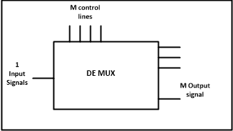
Demultiplexer
Pin Diagram
3.use 1-
to-4 Demultiplexer:
The 1-to-4 demultiplexer
has 1 input bit, 2 control bit, and 4 output bits. An example of 1-to-4
demultiplexer is IC 74155. The 1-to-4 demultiplexer is shown in figure below-
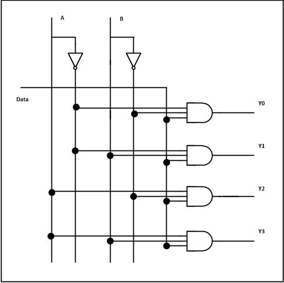
The input bit is
labelled as Data D. This data bit is transmitted to the data bit of the output
lines. This depends on the value of AB, the control input.
When AB = 01, the
upper second AND gate is enabled while other AND gates are disabled. Therefore,
only data bit D is transmitted to the output, giving Y1 = Data.
If D is low, Y1 is
low. IF D is high,Y1 is high. The value of Y1 depends upon the value of D. All
other outputs are in low state.
If the control input
is changed to AB = 10, all the gates are disabled except the third AND gate
from the top. Then, D is transmitted only to the Y2 output, and Y2 = Data.
Example of 1-to-16
demultiplexer is IC 74154 it has 1 input bit, 4 control bits and 16 output bit.
4.Practice Applications of Demultiplexer:
1. Demultiplexer is
used to connect a single source to multiple destinations. The main application
area of demultiplexer is communication system where multiplexer are used. Most
of the communication system are bidirectional i.e. they function in both
ways (transmitting and receiving signals). Hence, for most of the applications,
the multiplexer and demultiplexer work in sync. Demultiplexer are also used for
reconstruction of parallel data and ALU circuits.
2. Communication
System –
Communication system use multiplexer to carry multiple data like audio, video
and other form of data using a single line for transmission. This process make
the transmission easier. The demultiplexer receive the output signals of
the multiplexer and converts them back to the original form of the data at the
receiving end. The multiplexer and demultiplexer work together to carry out the
process of transmission and reception of data in communication system.
3. ALU (Arithmetic Logic
Unit) –
In an ALU circuit, the output of ALU can be stored in multiple registers or
storage units with the help of demultiplexer. The output of ALU is fed as the
data input to the demultiplexer. Each output of demultiplexer is connected to
multiple register which can be stored in the registers.
4. Serial to parallel converter –
A serial to parallel converter is used for reconstructing parallel data from
incoming serial data stream. In this technique, serial data from the
incoming serial data stream is given as data input to the demultiplexer at the
regular intervals. A counter is attach to the control input of the
demultiplexer. This counter directs the data signal to the output of the
demultiplexer where these data signals are stored. When all data signals have
been stored, the output of the demultiplexer can be retrieved and read out in
parallel.
Use circuit from web and use them
5. Major Project
Automatic Solar Tracker
Subject :A sample Project
on Digital Control System
Object: Increasing the
existing efficiency of the solar power by obtaining constant voltage output.
1.
Affordable
and efficient solution. Hence, an autonomous semi-portable solar power system
is constructed to supply power to a standard-sized home or remote areas.
2.
The
key aspects of this product are that it is affordable, efficient, standalone,
relatively easy to transport, and ready to use.
Theory:
1.
Solar
energy as an important renewable source of energy.
2.
The
efficiency of the solar system is
considerably low than that of typical energy sources.
3.
One
of the main cause of low efficiency is the variation of the light intensity
with time in an specified place.
4.
Solar
tracking is like the simple phenomenon analogous to that of sunflower
(heliotropism).
5.
Directing
the solar panel towards the area of high sunlight intensity.
Tool And Materials
1.
The
system’s main purpose is to efficiently harness solar energy and convert the
energy in a useful form for common domestic appliances and devices.
2.
The
system is fully autonomous.
3.
It
provides the simple automatic control unit that increases the efficiency of the
solar energy.
4.
It
uses simple operational amplifier ICs , resistors, photodiodes and motor
actuators as control unit.
Component:
1.
Photodiode:
1.
Light
dependent current/voltage source.
2.
It’s
a simple light sensor converting light energy to electrical energy.
3.
A
semiconductor device having PN junction.
4.
The
output is maximum when radiation flux is normal.
2. Operational Amplifiers
1.
One
of the most versatile electronic device. 
a.
Its
an high gain electronic voltage amplifier.
b.
It
is used for the purpose of low voltage signal amplification to usable signal.
c.
Its
one application is differential amplifier
which amplifies the difference of input signals.
d.
The
values of input resistors and feedback resistors can be so adjusted to maintain
the gain.
3. Resistors
1.
Various
resistors are used for current and voltage limiting purposes.
4. DC Stepper motor
1.
It
rotates clockwise and anticlockwise as the potential on it remains positive and negative accordingly.
2.
When
no voltage drop on motor, it will be stationary.
3.
The
motor is directly coupled to the solar panel so that as it rotates, the panel also rotates.
Working Principal


2.
The
diversion of the panel for maximum light intensity limit create noticeable
voltage difference between the diodes.
3.
The
output voltages are amplified individually and fed to differential amplifier
and finally to the motor.
4.
Finally
motor adjusts the panel towards the maximum light intensity direction i.e.
solar tracking
Figure
Conclusion
1.
The
voltage difference between the diodes makes to rotate the motors.
2.
The
magnitude and direction of motor depends upon the magnitudes of voltage on the
individual photodiodes.
3.
The
motor adjusts the tracker in desired location.
4.
Hence,
simple electronic devices and sensors can be used for the solar tracking
purpose representing an important and dynamic control system.
5.
It
can be used in robotics for robot way tracking process.
6.
It
can be upgraded in space missions.
7.
It
can be upgraded in automated cars and other vehicles too.
End
Computing tips ज्ञान-
क)Back up create:-
1.F b to
2.setting
infornation...post,vido..जे चाहिन्छ yes no tick
..a copy inf be created बने पछि
choose location,c.d....
3.download.
save folder.
ख)Rename:
1. select by ctrl/shift
2: Click F2
3: Enter name
4: click Enter(सवकाे नाम १---भई फेरिन्छ)
ग))Professinol...ल्बग कसरी पढ्ने?
1)Add google ID/email id(तपाईकाे)
2)Enter the email password.(")
3)At last log-in.ok पढ्नु ।
Creat photo album:-(माेवाईलमा)
1.select your photo from drive.
2.go collage,creativity,arrange them.(फ्रेम राेज्नुहाेस)
3.save.(अब तपाईले छानेकाे फाेटाेहरु एकै फाेटाेमा अाउछ)
Comments
Post a Comment